
2026-07-15
Thin-Film Deposition Equipment Outlook: AI Compute and Memory Upgrades Propel PECVD and ALD into a New Growth Cycle
Afilm Industry Insights | July 2026
Thin-Film Deposition Equipment Outlook: AI Compute and Memory Upgrades Propel PECVD and ALD into a New Growth Cycle
A frontline view from Afilm:
from SEMI data to 3D device architectures, decoding the new cycle in thin-film deposition equipment
INTRODUCTION
As a manufacturer specializing in thin-film deposition equipment such as PECVD (Plasma-Enhanced Chemical Vapor Deposition) and ALD (Atomic Layer Deposition), we continuously track the pulse of the global semiconductor equipment market. Since the second half of 2025, four mutually reinforcing threads — the AI compute build-out, the 3D transformation of memory devices, the ramp of advanced packaging, and domestic substitution in China — have been propelling thin-film deposition equipment into a new growth cycle. Drawing on public information from SEMI, industry research firms, and leading international vendors, this article reviews the key trends and shares our observations and responses. All data cited herein come from public sources with attribution; all charts were independently drawn by Afilm based on public data.
1
Global Market: Equipment Investment Rises; Mainland China Remains the Largest Market
According to data released by SEMI, global semiconductor equipment sales are expected to reach US$145 billion in 2026. Mainland China’s fab expansion momentum remains strong: semiconductor equipment sales reached US$14.56 billion in Q3 2025, keeping China the world’s largest market. As AI compute demand continues to surge and fab utilization stays high, equipment orders are showing clear structural volume growth.[1]
Domestic Chinese equipment makers delivered equally impressive results: according to Guosheng Securities, selected domestic equipment companies posted combined revenue of RMB 24.88 billion in Q3 2025, up 37% year over year, with a 2020–2024 revenue CAGR of 42% — significantly outpacing the global market as a whole.[2]
Our observation: unlike past cyclical restocking, this round of equipment investment is driven by structural capacity gaps created by AI servers, HBM, and advanced packaging. For equipment vendors, both order visibility and order durability are improving.
2
Thin-Film Deposition Equipment: A US$28 Billion Market Keeps Expanding, with ALD Growing Fastest
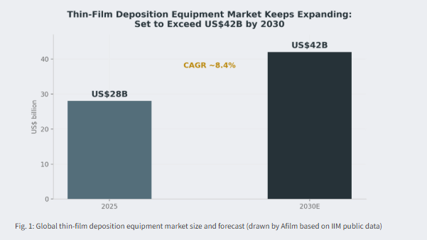
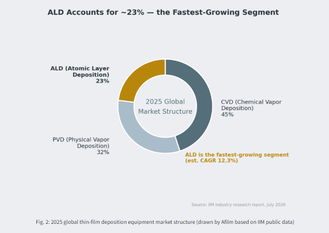
Thin-film deposition is one of the most step-intensive process segments in IC manufacturing. A report from industry research firm IIM shows that the global thin-film deposition equipment (CVD/PVD/ALD) market exceeded US$28 billion in 2025, with CVD accounting for roughly 45%, PVD roughly 32%, and ALD — at about 23% — the fastest-growing segment. The global market is expected to surpass US$42 billion by 2030, with ALD equipment projected to grow at a 12.3% CAGR. Demand in China reached US$8.2 billion in 2025, up 19.7% year over year, driven mainly by foundry capacity expansion and the ramp of advanced memory devices.[3]
By market structure, CVD (including PECVD, LPCVD, and others) remains the largest technology route, while ALD — thanks to its atomic-level thickness control and excellent step coverage — is becoming the fastest-growing segment in advanced process nodes.
3
Structural Opportunities: 3D Device Architectures, HBM, and Advanced Packaging
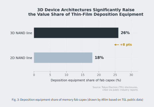
The 3D transformation of memory devices is directly amplifying the value of thin-film deposition equipment. Tokyo Electron (TEL) has disclosed that deposition equipment’s share of Flash fab capex has risen from 18% in the 2D era to 26% in the 3D era; as 3D NAND stacking moves beyond 500 layers, deposition steps will increase accordingly. SEMI forecasts global memory-related equipment spending of US$136 billion for 2026–2028, with 3D NAND accounting for more than 40% of the total; the HBM boom is also driving significant demand growth for lithography, ALD, bonding, and other equipment.[4]
Recent moves by leading international vendors corroborate this trend: in February 2026, Applied Materials unveiled deposition and materials engineering systems for the 2nm node and below at SEMICON Korea 2026; in September 2025, Lam Research partnered with JSR and Inpria to accelerate the development of next-generation materials for ALD processes. Equipment–material co-innovation is becoming the new focal point of competition in advanced deposition technology.[5]
4
Domestic Substitution: A Window from “Replacement” to “Leadership”
Driven by both external conditions and endogenous demand, domestic thin-film deposition equipment is breaking through at an accelerating pace. We believe domestic substitution has moved beyond point-by-point "replacement" into a phase of systematic competition: customers' evaluation of domestic tools is shifting from "whether they work" to "whether they work well, run stably, and deliver a better total cost of ownership." This raises the bar for equipment vendors' process know-how, mass-production consistency, and service capability — and it is precisely where vendors with genuine technical depth can pull ahead.
5
Afilm’s Observations and Positioning
As a manufacturer focused on thin-film deposition equipment such as PECVD and ALD, we have formed two judgments based on continuous tracking of customer demand:
—PECVD has the most certain demand. In advanced packaging and mature-node expansion, dielectric thin-film deposition is used in large volumes within mature process windows; customers care most about throughput, stability, and TCO. Afilm’s PECVD series keeps iterating on film-thickness uniformity, particle control, and throughput efficiency, covering logic, memory, and advanced-packaging applications.
—Equipment–process co-delivery is the watershed. Customers no longer want an isolated tool but an integrated “equipment + process solution + rapid response” delivery capability. Afilm has built a full-cycle service system spanning pre-sales process evaluation, installation and commissioning, and volume-production support.
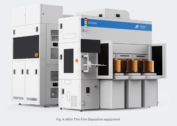
Looking ahead to the second half of the year, the visibility of the AI compute build-out and memory expansion remains strong, and the momentum of thin-film deposition equipment is expected to continue. Afilm will keep increasing R&D investment in core PECVD and ALD technologies and — with more stable equipment performance and process services closer to customers — work with partners across the value chain to capture this growth cycle.
Sources & Attribution
The data and factual information in this article come from the following public channels: SEMI public data and industry commentaries; IIM, Global and China Thin-Film Deposition Equipment (CVD/PVD/ALD) Industry Value Chain Research and Analysis Report (July 2026); Tokyo Electron (TEL) public disclosures; excerpts from Guosheng Securities and Donghai Securities research reports; industry coverage by PEdaily (a Zero2IPO media outlet); and public releases from Piotech, AMEC, NAURA, Leadmicro, and other companies. All data are attributed in the text or in the footnotes.
Figures 1–3 were independently drawn by Afilm based on the above public data; the copyright therein belongs to Afilm.
Source
[1]SEMI, cited via Guosheng Securities industry commentary and public financial media coverage, March 2026.
[2]Guosheng Securities statistics, cited via public financial coverage, March 2026.
[3]IIM, Global and China Thin-Film Deposition Equipment (CVD/PVD/ALD) Industry Value Chain Research and Analysis Report, July 2026.
Copyright & Disclaimer: This article was originally written by the Afilm Marketing Department for industry exchange only and does not constitute investment advice. Third-party data cited herein are attributed to their sources; if you are a rights holder of any cited data and have questions about its use, please contact us and we will verify and address it promptly. For reprint authorization, please contact the Afilm Marketing Department.
