
2026-09-04
Gap-Fill Equipment Outlook: Reassessing the Value of SACVD and Combined Gap-Fill Solutions Amid Process Scaling
Afilm Industry Insights | September 2026
Gap-Fill Equipment Outlook: Reassessing the Value of SACVD and Combined Gap-Fill Solutions Amid Process Scaling
Applied Materials' long-held dominance is loosening, and domestic tools are finding their opening in
mature-node expansion
INTRODUCTION
As a manufacturer specializing in thin-film deposition equipment such as PECVD and ALD, we noticed — while tracking the evolution of dielectric deposition technology — that SACVD (Sub-Atmospheric Chemical Vapor Deposition), a relatively low-profile niche category, has recently regained attention on the back of volume orders for domestic tools and topical reports from several research firms. This article reviews SACVD’s technical positioning, Applied Materials’ competitive landscape, and the progress of domestic substitution, and shares our judgment on where gap-fill equipment is heading. All data cited herein come from public sources with attribution; all charts were independently drawn by Afilm based on public data.
1
Understanding SACVD: A Deposition Technology Born for Gap Fill
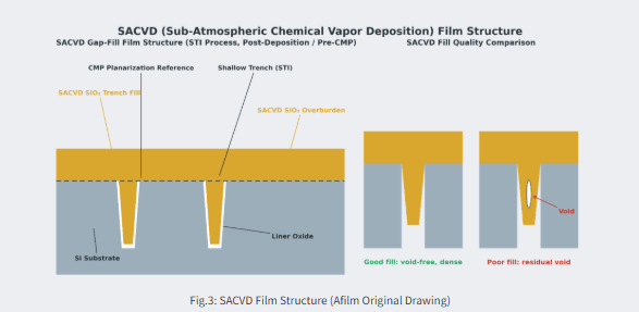
SACVD (Sub-Atmospheric CVD) deposits dielectric films through thermal reaction at roughly 400–550°C under sub-atmospheric pressures of 30–600 Torr; typical films include BPSG (borophosphosilicate glass), SAF, and SA-TEOS. Its high reactant concentration and elevated temperature deliver excellent step coverage and gap-fill capability, making it the workhorse technology for trench-fill processes such as STI (Shallow Trench Isolation) and ILD/PMD (Inter-Layer / Pre-Metal Dielectric), performing best at aspect ratios up to 7:1.[1]
Unlike PECVD, which relies on plasma enhancement, SACVD deposits purely through thermal reaction and offers excellent film-stress and impurity control — especially suited to fill-quality-sensitive structures with moderate aspect ratios. In STI isolation for logic chips and in dielectric layers for power devices and CIS (CMOS image sensors), SACVD has long been an irreplaceable standard process.
2
Competitive Landscape: Applied Materials Dominates; Domestic Vendors Go from Zero to One
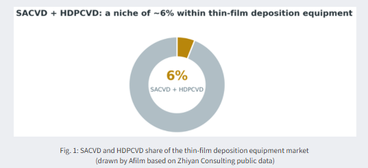
By market size, SACVD is a niche category: according to Zhiyan Consulting, SACVD and HDPCVD together account for roughly 6% of the thin-film deposition equipment market. Given the limited category size, equipment vendors typically do not disclose SACVD product-line revenue or share separately, so the competitive landscape must be inferred from adjacent businesses.[2]
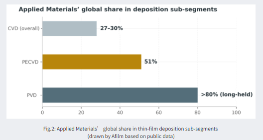
Globally, the SACVD market has long been dominated by Applied Materials (AMAT), Lam Research, and Tokyo Electron (TEL), with AMAT’s Producer SACVD regarded as the industry benchmark. Applied Materials does not disclose SACVD share separately, but the circumstantial evidence is ample: its overall global CVD share is about 27%–30%, its PECVD share reaches 51%, and its PVD share has long stayed above 80% (2022 data). More importantly, since its launch in 1998, the Producer platform has become the base platform for depositing a wide range of materials — covering 150–300mm wafers and serving logic, DRAM, and NAND, as well as MEMS, optoelectronics, and power devices — and SACVD is one of the platform’s flagship process modules.[3]
Afilm has also built a strong presence in SACVD equipment. Its 12-inch GFF (Gap-Fill Film) tool is a system developed by AFilm for STI (Shallow Trench Isolation) applications at the 28nm node and below. For silicon oxide film processes, it delivers void-free gap fill at an aspect ratio of 8:1 — an industry-leading capability.
3
Technology Trend: Rising Aspect Ratios; Single Technologies Give Way to Combined Solutions
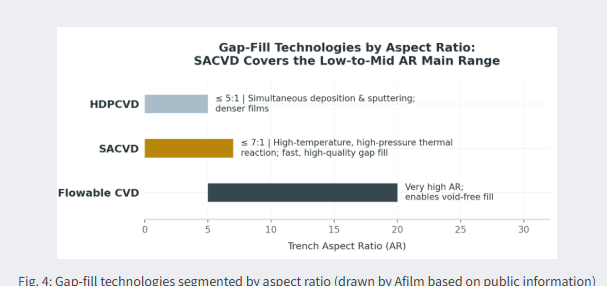
Process scaling makes device trenches deeper and openings narrower, raising the bar for fill uniformity, film density, and defect-freeness; no single fill technology can cover every scenario. The industry is converging on combined solutions segmented by aspect ratio: HDPCVD, with simultaneous deposition and sputtering, yields denser films and suits aspect ratios up to 5:1; SACVD relies on high-temperature, elevated-pressure thermal reaction for fast, high-quality gap fill, covering the main battleground up to 7:1; and Flowable CVD targets extremely high aspect ratios, enabling void-free fill.
4
Demand Trend: Mature-Node Expansion Is the Base Market; Domestic Substitution Opens a Window
SACVD’s main battleground is the 40/28nm nodes and above — corresponding to logic, power, analog, CIS, and memory periphery circuits — exactly where mainland China is expanding capacity most aggressively today. Continuous mature-node expansion gives SACVD a stable and predictable demand base.
At the landscape level, export controls restrict sales of advanced deposition equipment to China, and domestic fabs are proactively opening qualification windows for domestic tools; AMAT’s SACVD share in China’s mature-node lines is being materially diverted to domestic equipment. Since 2025, research firms including QYResearch and Gelonghui have published dedicated SACVD equipment market reports covering 2020–2031 shipment and revenue trends — the fact that a niche category is being studied on its own itself reflects rising market attention. Globally, Applied Materials’ dominance is unlikely to be shaken in the near term, but in China a structural substitution of “mature nodes + domestic qualification” has already begun.
5
Afilm’s Observations
As a manufacturer focused on thin-film deposition equipment such as PECVD and ALD, we have formed three judgments based on continuous tracking of the SACVD segment:
—SACVD is a platform process module, not a standalone category. A roughly 6% market share means it can hardly support an independent product line; but as a capability piece in the dielectric-deposition platform puzzle, it directly shapes customers’ assessment of a vendor’s overall delivery capability. AMAT’s Producer platform model — and Piotech’s path of deriving SACVD from its PECVD platform — both bear this out.
—Platform synergy with PECVD is a natural entry point. SACVD and PECVD share substantial platform technologies — vacuum, wafer transfer, temperature control — so vendors with existing PECVD know-how have a realistic basis for extending into gap-fill process packages such as SA-TEOS and BPSG. The plasma control, film-thickness uniformity, and particle control capabilities that Afilm has accumulated on its PECVD platform can be reused in developing gap-fill processes.
—Customer value points are clear: fill quality, stability, and TCO. Mature-node customers’ core demand for domestic tools has shifted from “usable” to “well-performing, stable, and worry-free.” Tools with void-free fill, excellent particle control, and long maintenance intervals will earn repeat orders — the key threshold for domestic SACVD to move from first-tool qualification to volume ramp.
In summary, SACVD’s standalone market space is limited, but the gap-fill capability it represents is becoming an important piece of platform-based competition among dielectric deposition vendors. Driven by both mature-node expansion and domestic substitution, vendors with platform technology reserves and process-synergy capabilities will take the initiative in this round of landscape reshaping. Afilm will continue to track the development of gap-fill technology and, with PECVD and ALD at its core, steadily expand the boundaries of its dielectric deposition process coverage.
Sources & Attribution
The data and factual information in this article come from the following public channels: Zhiyan Consulting (SACVD/HDPCVD market share, 2023); Gartner and other market-share data (cited via CICC Research and public industry materials, 2022); Applied Materials official public product materials; Piotech official public materials and Donghai Securities research excerpts (January 2026); and SACVD equipment market research reports from QY Research, Gelonghui, and others (2025–2026). All data are attributed in the text or in the footnotes.
Figures 1–4 were independently drawn by Afilm based on the above public data; the copyright therein belongs to Afilm. Applied Materials, Lam Research, Tokyo Electron (TEL), Piotech, and other names are trademarks or trade names of their respective owners and are referenced herein solely for industry information purposes.
Source
[1]public SACVD process technical materials and industry research reviews, 2025–2026.
[2]Zhiyan Consulting, 2023.
[3]Gartner et al., cited via CICC Research and public industry materials, 2022; Applied Materials public product materials.
Copyright & Disclaimer: This article was originally written by the Afilm Marketing Department for industry exchange only and does not constitute investment advice. Third-party data cited herein are attributed to their sources; if you are a rights holder of any cited data and have questions about its use, please contact us and we will verify and address it promptly. For reprint authorization, please contact the Afilm Marketing Department.
