
中文版 English
  • +About Us
    Company Profile
    Afilm Culture
    Afilm Qualification
    ESG
    System & Product Qualifications
    Honors
    Intellectual Property
  • +News
    News
    Industry News
  • +Products & Service
    CVD
    ALD
    UV Cure
    Service
    PECVD
    SACVD
    HDR
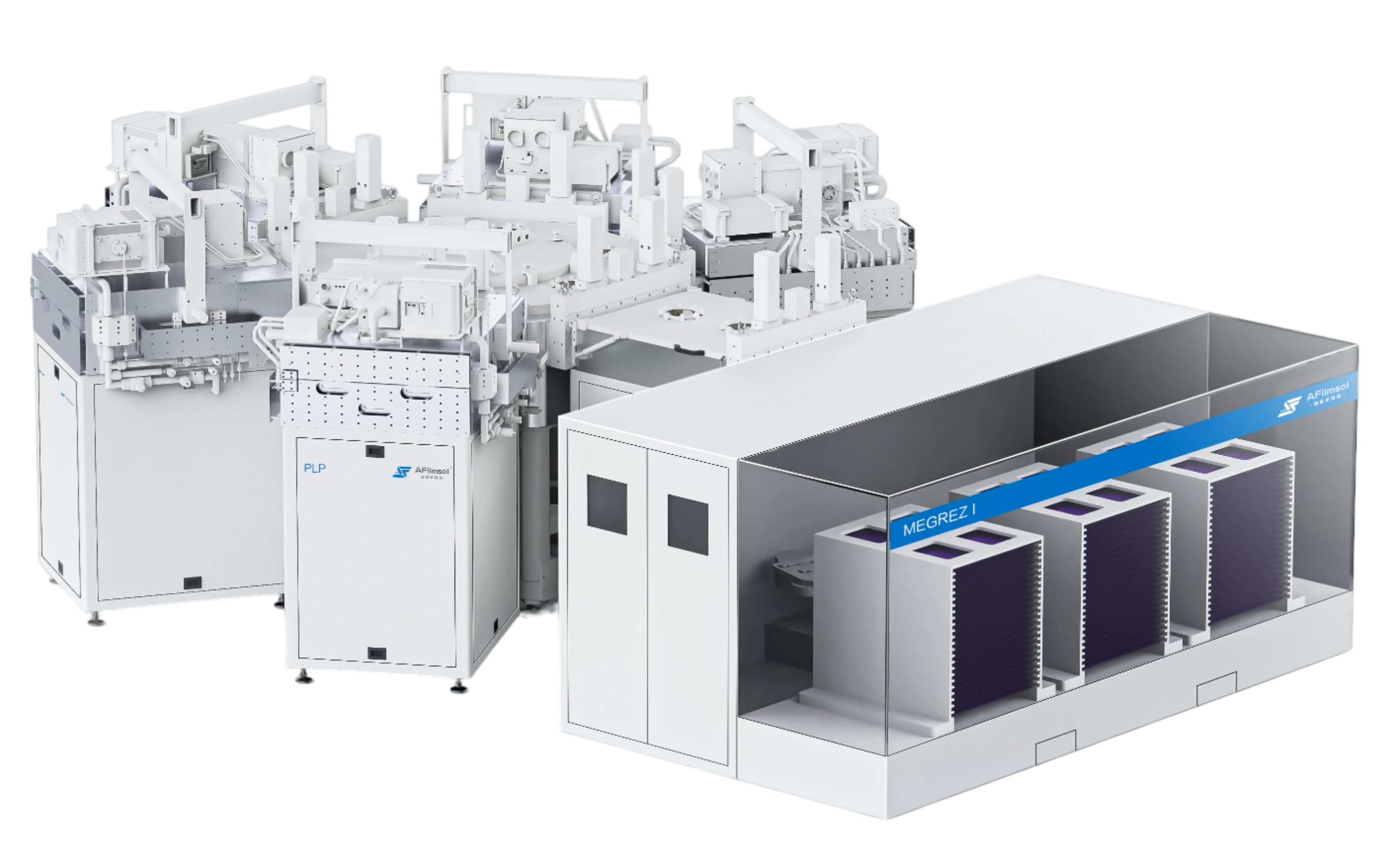
    PLP
  • +Careers
    Compensation & Benefits
    Campus Recruitment
    Social Recruitment
  • +Contact Us
  • Language: 中文版 English

Provide the excellent film deposition equipments and solutions. Provide the excellent film deposition equipments and solutions. Provide the excellent film deposition equipments and solutions. Provide the excellent film deposition equipments and solutions.

Products

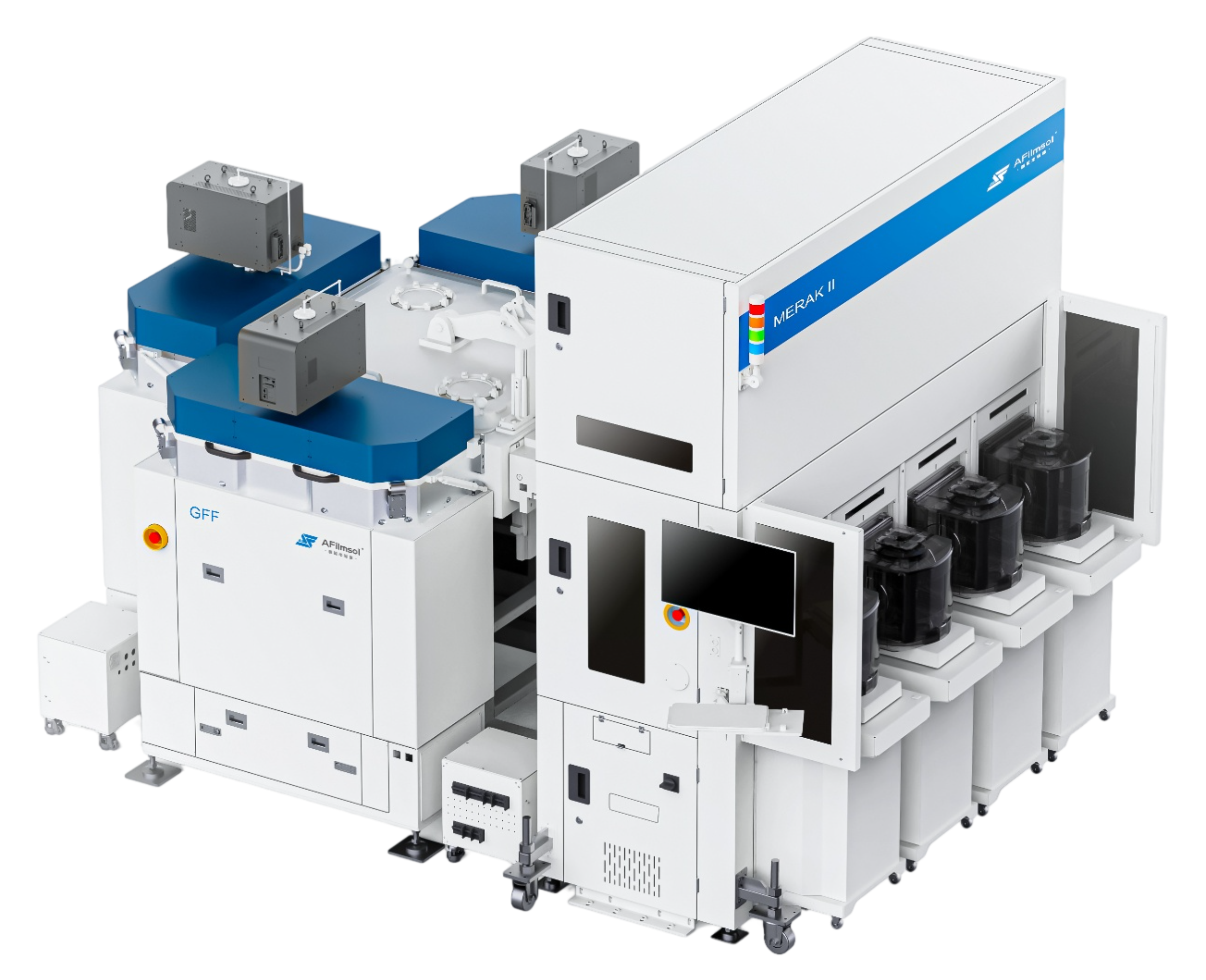
  • CVD

  • ALD

  • UV Cure

News

2026-09-04

Gap-Fill Equipment Outlook: Reassessing the Value of SACVD and Combined Gap-Fill Solutions Amid Process Scaling

2026-07-15

Thin-Film Deposition Equipment Outlook: AI Compute and Memory Upgrades Propel PECVD and ALD into a New Growth Cycle

2026-07-09

Afilm Semiconductor — China's Potential Unicorn Enterprise

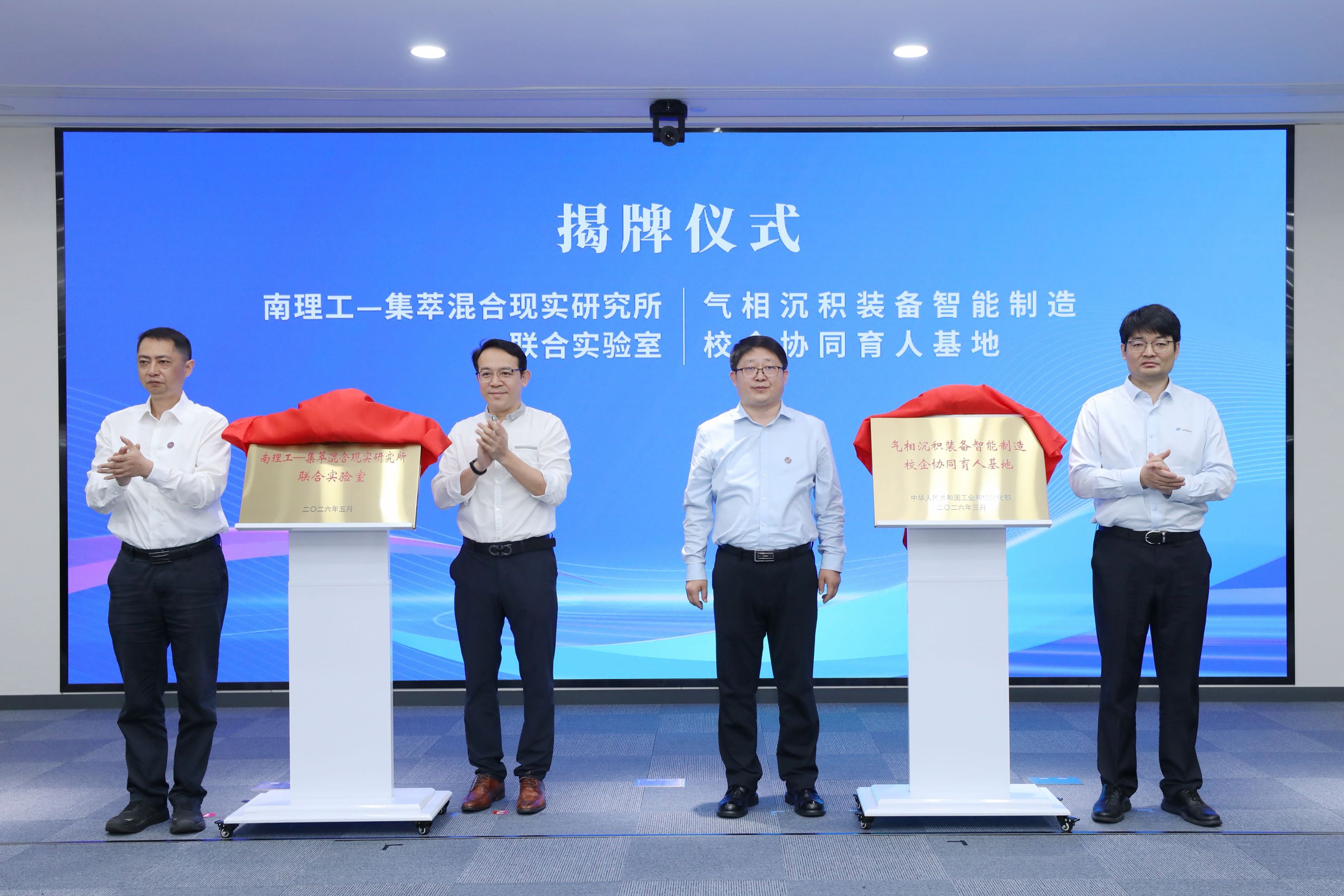
2026-05-21

“Double High Collaboration” Aggregates the Force | Afilm Semiconductor Joins MIIT Accredited Industry-University Collaborative Education Base Development

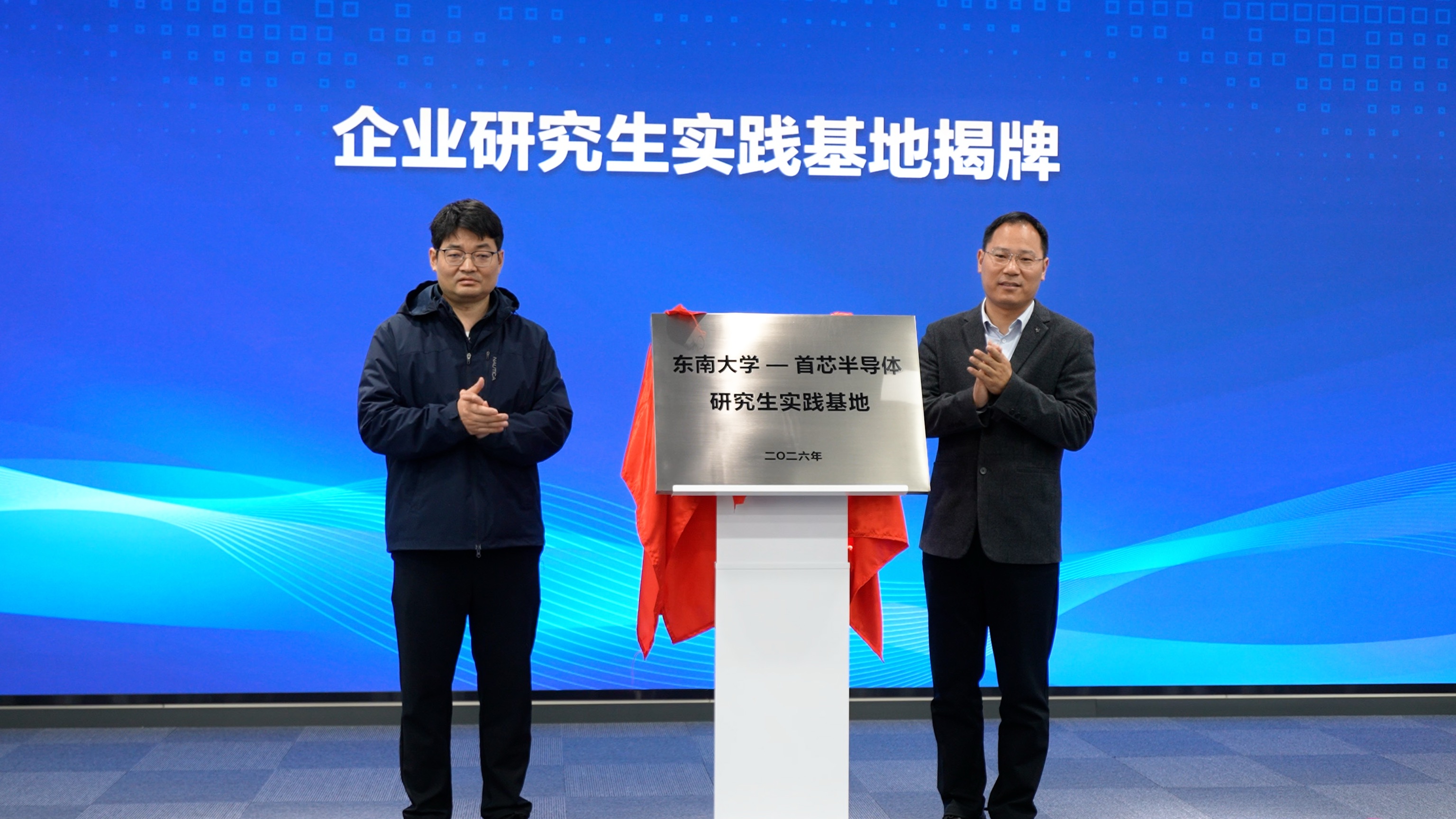
2026-04-15

Officially Unveiled the Southeast University – Afilm Semiconductor Graduate Practice Base

2025-12-31

Afilm Semiconductor Completed a New Round of Financing, Receiving Joint Support from the New and Existing Investors as well as Provincial Special Funds

About us
News
Products & R&D
Careers

COPYRIGHT © 2024 Jiangsu Afilm Semiconductor Technology Co. Ltd  ALL RIGHTS RESERVED.

SHARE US: